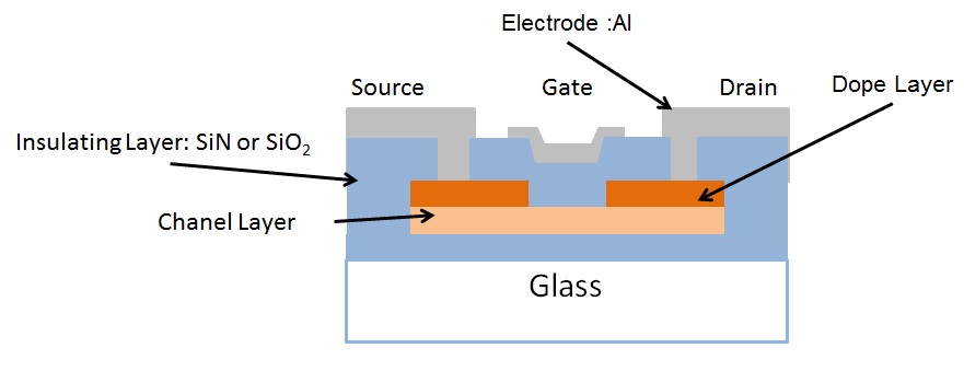
薄膜トランジスタ(TFT)
TFT device
TFTs (Thin Film Transistors) are used as switching device in LCD (Liquid Crystal Display).
TFT is a kind of FET (Field-Effect Transistor), but is formed on glass panel not in the Si wafer.
In our lab, research on the process and the device-simulation of poly Si TFT is done.
As the Si film deposition, mainly, sputtering technique is used.
TFT fabrication process is formed by repeating the process of deposition, patterning, etching and cleaning etc. at each layer.
Not only un-doped Si but also P- or B-doped Si, and even SiO2 film can be deposited using RF sputtering.
High quality poly Si films are was made realized as a result of original annealing techniques such as rapid thermal annealing or laser annealing.
結晶化
Aiming to realize TFTs on flexible panel such as plastic or thin glass, research on new and original crystallization using low temperature process is conducted.
Crystallization of sputtered a-Si thin films on glass is tried by using solid phase grain growth and laser annealing.
Insulation film
In the high performance thin film transistor, it is important to form a good high quality gate insulation film.
The characterization of the films formed by made of the RF spatter is done.
The thermal annealing effects including laser annealing are studied.
The research target is improves the electric strength, and the reduction of leak current.
The following techniques can be availlable as evaluation tools.

Laboratory Information
【野口研究室】
![]() TEL +81-98-895-8680
TEL +81-98-895-8680
![]() FAX +81-98-895-8708
FAX +81-98-895-8708
〒903-0213 沖縄県西原町千原1番地